Overview
|
In this assignment we were to make a circuit that we could use to display our birth date on a seven segment display by toggling three switches. the seven segment had to be a common cathode and use resistors to make sure that the display didn't get over powered.
|

|
Truth Table
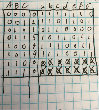
|
By creating the truth table we can figure out the necessary outputs for each segment to work correctly. A B and C represent the three switches used to toggle the circuit and a through g represent each of the seven segments on the display. The X's represent conditions where the outcome doesn't matter since we are only concerned with the first 6 numbers. the numbers shown in the unlabeled column are the digits that are supposed to be displayed according to which switches are toggled.
|
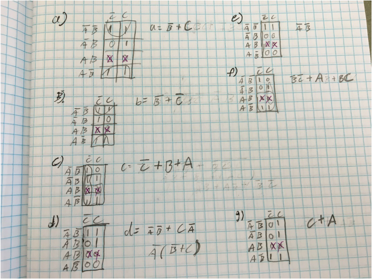
Karnaugh Maps
|
K-mapping is a very useful tool for helping us get simplified logic expressions without using Boolean algebra. You do this by circling groups of 1 and or X's and writing down the common terms that they share. The expressions are all obtained in the sum of products form and I kept them all in that form except for segment d which was easier to wire in the product of sums form. By using X's, you can make larger circles on the K-maps, this allows for simpler circuits.
|
|
MultiSim Implementation
|
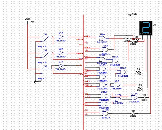
This circuit was created using MultiSim. The 74ls00 gates represent NAND gates, 74LS04 represents inverters, 74LS08 represents AND gates, and the 74LS32 represents OR gates.
This circuit is in bus form and uses 4 different types of chips. It had 3 inverters, 2 NAND gates, 4 AND gates, and 8 OR gates. Therefore I need one of each of 74LS00, 74LS04, and 74LS08 and I need 2 74LS32 chips. I used a NAND circuit on the e segment because I had to use it somewhere but it was simplest to use it there. I could have used only one AND gate but either way i would have used the same number of chips. NAND and NOR gates allow you to use less gates than an AOI circuit. In this circuit I used a common cathode for no specific reason. the only difference between the cathode and anode is that the cathode had to be grounded whereas the anode must be connected to a power source. The resistors are there to prevent a segment form lighting up when it shouldn't. |
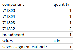
Table of materials
|
This table shows the list of materials needed to create my birthday display circuit. I did not get a chance to count the number of wires but I probably used around 30 to 40 wires.
|
|
Breadboarding
First I placed all the chips on the board and grounded and powered. The chips are laid in numerical order according to the last two numbers of each chip.
|
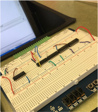
This is about halfway through breadboarding all the segments. the chip all the way to the left is the NAND chip.
|
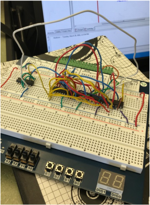
This is the final circuit and has been tested and works the way it should.
|
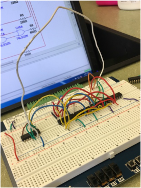
My second time bread boarding was almost entirely trouble free and it worked the first time. One thing I realized while making this circuit is that the entire row that the output is on can be used to show that output. For example, if the output is not A, the entire row can be used as not A. i laid out the pins numerically and it worked out pretty well but it was fairly cluttered around the OR gates. next time I would leave more space between the chips.
Conclusion
This project helped me better understand how to breadboard efficiently and also the importance of k-mapping. I learned new techniques such as using an output multiple times. I also tried to color coordinate the board but ran out of wires of most of the colors and all I had to use were red, yellow, blue, and white wires. I'm still not entirely sure how the integrated circuits work. I understand how to use them but I don't really know what separates each chip in terms of their function. K-mapping is extremely useful and allows you to get the logic expression without going through long Boolean algebra processes. Sometimes I forget to switch the 3rd and 4th rows when I move the outputs from the truth table to the K-map.
