
|
Project OverviewIn this project we were tasked with creating a display that counted up to 80 and stops. There also had to be a reset button that went back to 0 no matter what number it was on.
|
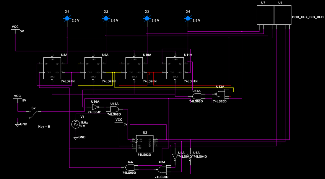
MultiSim Circuit
PLD Circuit
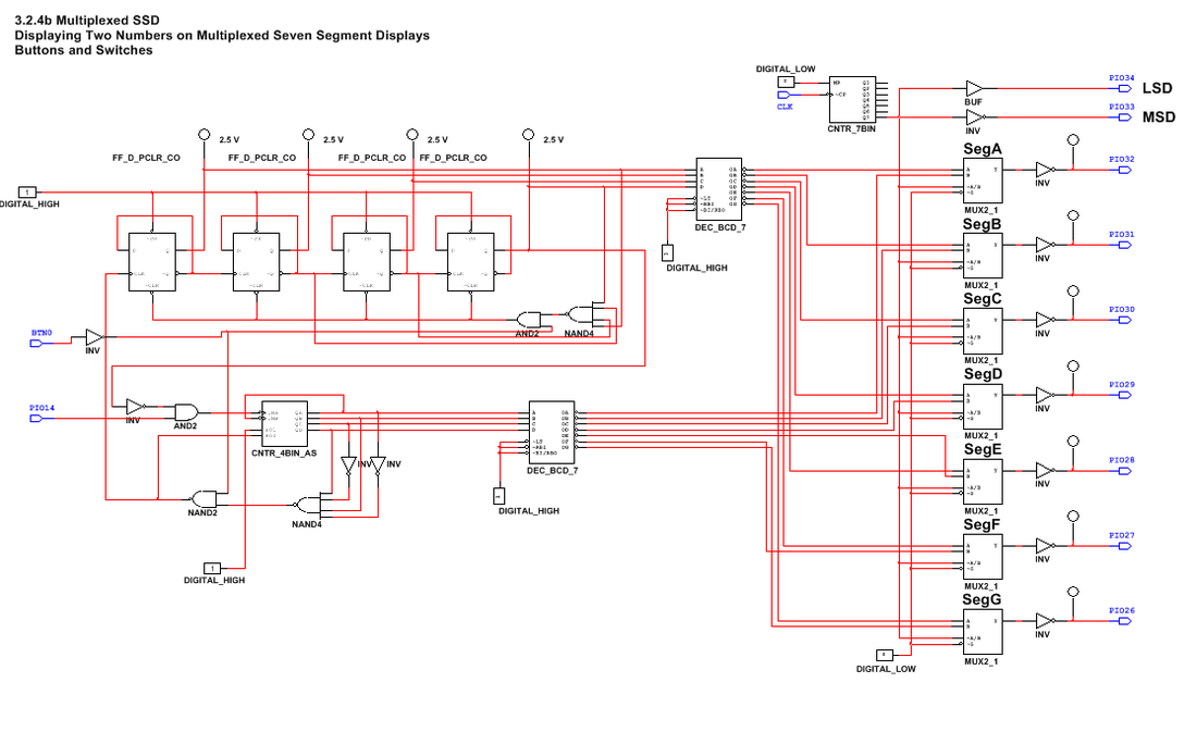
The biggest difference between PLD mode and Design mode is pin assignment in which you assign inputs and outputs to pins. Rather than designing a switch to use to go back and forth between power and group, you can simply replace it with an input connection such as the button built into the PLD chip. outputs are a little less convenient. For example, rather than wiring outputs to a seven segment display in multisim, you have to assign each output to a pin on the PLD chip and wire that pin to the corresponding input on the breadboard. Uploading the circuit is fairly easy once you find the right file. You also need to use NI Elvis to run the clock and make the circuit work.
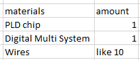
Bill of Materials
Final Project Conclusions
1. SSI uses chips like the 74LS04 when bread boarding whereas MSI uses one large chip that can do many different functions like the PLD chip
2. Due to the use of the 4 digit binary counter, I cannot make the circuit start at any digit other than 0.
3. The ripple effect is the slight delay between digits on the display due to using multiple flipflops.
4. On the up switch of the clock, the 74LS93 chip detects a signal and adds one to its count, this is displayed on the LSD display. when this count reaches ten, it is detected by the 4 input NAND gate and then again by a second NAND gate. The output from the NAND gate is then sent to the RO2 input which causes the LSD circuit to reset to zero. However, the NAND gate also sends a positive signal to the clock input of the first 74LS74 chip, causing the MSD circuit to register a 1. this is displayed on the MSD hex display. Every time the LSD circuit reaches ten, another signal is sent to the MSD circuit, causing its count to increase by 1. When the top circuit has reached an 8, it sends a signal from the Q output of the fourth '74 chip, this positive signal is inverted to a low signal which prevents the clock's signal from passing through the AND gate, thus pausing the circuit. The reset switch acts by sending a low signal to the clears of the MSD circuit and by sending a high signal to the RO2 input on the '93 chip.
5. some students had an inverted after their reset switch. this caused the circuit to only work while the reset switch was pressed and would reset as soon as it was let go.
